 英语
英语 西班牙语
西班牙语 德语
德语TableCUT-200 Automatic Precision Cut-Off Machine
Product Description
TableCUT-200 is automatic precision cut-off machine, equipped with various fixtu...
We use first- and third-party cookies including other tracking technologies from third party publishers to give you the full functionality of our website, to customize your user experience, perform analytics and deliver personalized advertising on our websites, apps and newsletters across internet and via social media platforms. For that purpose, we collect information about user, browsing patterns and device.
By clicking "Accept All Cookies", you accept this, and agree that we share this information with third parties, such as our advertising partners. If you prefer, you can choose to continue with "Only Required Cookies". But keep in mind that blocking some types of cookies may impact how we can deliver tailored content that you might like.
For more information and to customize your options, click on "Cookie settings". If you want to learn more about cookies and why we use them, visit our Cookie Policy page at any time. Cookie Policy

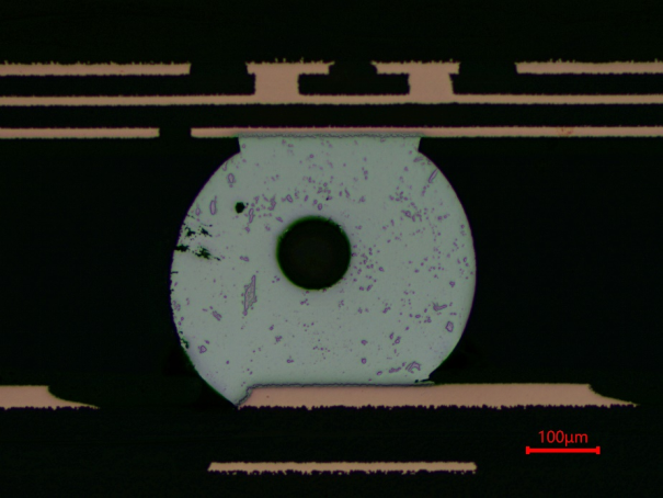
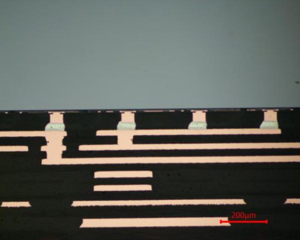
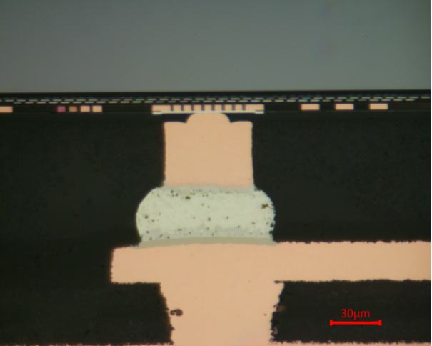
As electronic products continue to evolve towards miniaturization and high-density integration, ball grid array (BGA) packaging has become the core packaging form for devices such as smartphones and aerospace systems due to its ability to achieve high I/O pin density connections. Although the solder joints between BGA and printed circuit boards (PCBs) are of tiny size (with diameters typically ranging from 0.3 to 0.8 mm), they are crucial nodes that maintain electrical signal conduction and mechanical structure stability. Their quality directly determines the long-term reliability of electronic devices. Therefore, PCBA slicing analysis has become the core method for inspecting BGA solder joint quality.
This analysis focuses on detecting the following three types of indicators:
PCBA slicing analysis can precisely trace the quality of solder joints, and is used not only for mass production screening but also for failure location assistance, serving as the core support for ensuring the functionality and integrity of electronic devices.
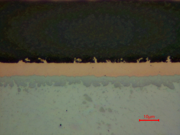
Here is an example of a BGA sample preparation plan for a solder joint approximately 80 μm in size. Please refer to the following plan for your reference:
1️⃣ : Use P1200 metallographic sandpaper to polish to the target position edge
2️⃣ : Use P2000 metallographic sandpaper to polish to the target position
3️⃣ : Use SC-JP polishing cloth and 3 μm diamond polishing liquid for polishing.
4️⃣ : Use ET-JP polishing cloth and 1 μm diamond polishing liquid for polishing.
5️⃣ : Use ZN-ZP polishing cloth and SO-A439 50-nanometer silica polishing liquid for final polishing.

.jpg?imageView2/2/w/400/format/jpg/q/75 "PL-W Polishing Lubricants")


Based in China, TROJAN pays attention to the international market, and has sold metallographic equipment to more than 50 countries, such as Europe, America, Japan and South Korea, Southeast Asia countries and regions


