 英语
英语 西班牙语
西班牙语 德语
德语Abrasive Wheels
Product Description
Cuting is the first step in material analysis, and the selection of the cutting ...
We use first- and third-party cookies including other tracking technologies from third party publishers to give you the full functionality of our website, to customize your user experience, perform analytics and deliver personalized advertising on our websites, apps and newsletters across internet and via social media platforms. For that purpose, we collect information about user, browsing patterns and device.
By clicking "Accept All Cookies", you accept this, and agree that we share this information with third parties, such as our advertising partners. If you prefer, you can choose to continue with "Only Required Cookies". But keep in mind that blocking some types of cookies may impact how we can deliver tailored content that you might like.
For more information and to customize your options, click on "Cookie settings". If you want to learn more about cookies and why we use them, visit our Cookie Policy page at any time. Cookie Policy

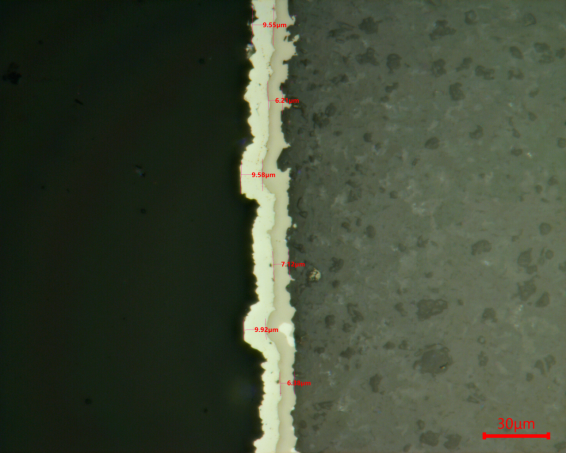
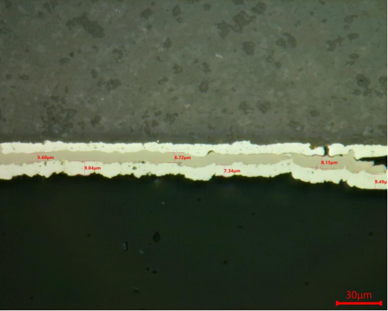
As a core passive component in the modern electronics industry, SMD Resistors (Surface Mount Device Resistors) are the “invisible workhorses” with the highest usage in electronic equipment. Featuring a lead-free design, they are directly mounted on circuit boards via surface mount technology (SMT). Constructed with an alumina ceramic substrate, paired with metal-glass glaze or vacuum-sputtered alloy resistor films, they are manufactured through precision processes.
Key advantages of this component: Compact size for high-density packaging, resistance to high temperatures and humidity, low temperature coefficient, and precision as high as ±0.01%. Widely used in consumer electronics, 5G base stations, automotive electronics, and other fields, they quietly perform critical functions such as current limiting and voltage division.
The structural morphology and dimensional specifications of the electroplated nickel and tin layers at both ends directly determine the long-term operational stability of the component. To clearly reveal the cross-sectional microstructure of these two layers, here’s a reference for the metallographic preparation process of SMD Resistors:
1️⃣ Grind to the edge of the target position using a P400 resin-bonded diamond grinding disc;
2️⃣ Fine grinding to the target position with a POS grinding disc + 9μm PD-WT polycrystalline diamond;
3️⃣ Rough polishing with SC-JP polishing cloth + 3μm PD-WT polishing slurry;
4️⃣ Final polishing with ZN-ZP polishing cloth + SO-T439 50nm polishing solution.
#Trojanmetallography #Metallography #ElectronicComponents #SamplePreparation #Trojan
.jpg?imageView2/2/w/400/format/jpg/q/75 "Abrasive Wheels")

.png?imageView2/2/w/400/format/jpg/q/75 "Disposable Sample Cups")
")
")


Based in China, TROJAN pays attention to the international market, and has sold metallographic equipment to more than 50 countries, such as Europe, America, Japan and South Korea, Southeast Asia countries and regions


