
 英语
英语 西班牙语
西班牙语 德语
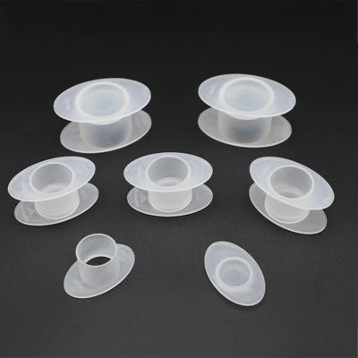
德语2-Part Mounting Cups
Product Description
The 2-part Mounting Cups feature a detachable bottom, allowing easy removal of ...
We use first- and third-party cookies including other tracking technologies from third party publishers to give you the full functionality of our website, to customize your user experience, perform analytics and deliver personalized advertising on our websites, apps and newsletters across internet and via social media platforms. For that purpose, we collect information about user, browsing patterns and device.
By clicking "Accept All Cookies", you accept this, and agree that we share this information with third parties, such as our advertising partners. If you prefer, you can choose to continue with "Only Required Cookies". But keep in mind that blocking some types of cookies may impact how we can deliver tailored content that you might like.
For more information and to customize your options, click on "Cookie settings". If you want to learn more about cookies and why we use them, visit our Cookie Policy page at any time. Cookie Policy

High‑power conductive copper busbars and integrated shunt resistors commonly adopt a dual‑layer electroplating structure: 1.5‑4μm nickel underlayer + 3‑8μm tin top layer, balancing corrosion resistance and electrical assembly requirements.
Acting as a barrier layer, the dense nickel underlayer blocks outward diffusion and oxidation of copper substrate ions. It improves plating adhesion, enhances wear‑resistant and high‑temperature‑resistant performance, and mitigates fretting corrosion under vibration. This makes it ideal for demanding applications such as energy‑storage systems, DC charging piles and vehicle‑mounted electronic controls.
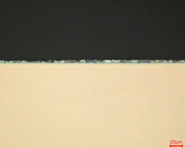
Figure 1: Cross-sectional overview of the dual-layer electroplated coating.
The outer tin coating delivers stable low contact resistance and excellent solderability. It deforms plastically under bolt compression, ensuring long‑term low‑thermal‑resistance performance at connection points.
Single tin plating suffers from Cu‑Sn interdiffusion, tarnishing and discoloration. Nickel‑only plating shows poor solderability. The combined nickel‑tin plating leverages strengths of both layers while avoiding their drawbacks. It is widely used in energy‑storage shunts, PV inverter busbars and high‑power new‑energy electrical connectors.
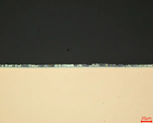
Figure 2: Interface morphology showing the transition between copper and coating layers.
Key challenge for metallographic preparation of Ni‑Sn double‑layer coated busbars & shunts: handling this alternating soft‑hard thin‑layer structure.
Precise control over three critical steps is essential:
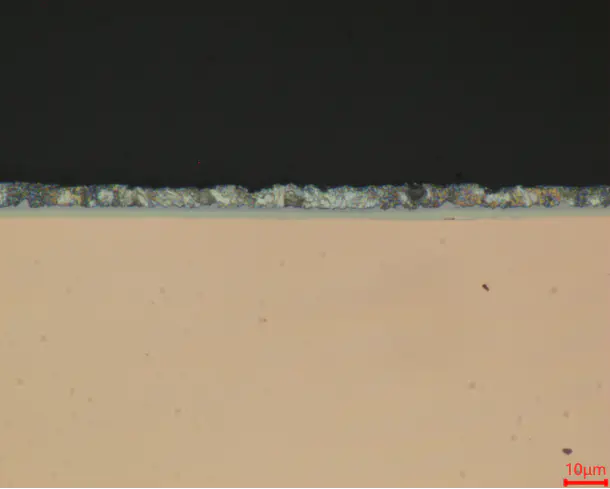
Figure 3: High-magnification layer thickness inspection.
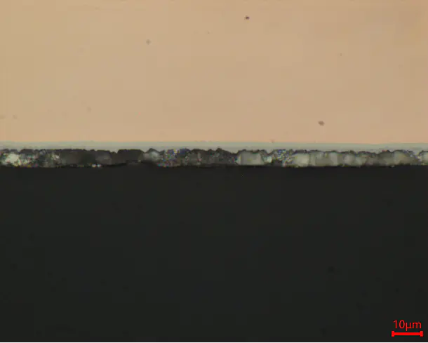
Figure 4: Fully prepared metallographic cross-section.
Standardized operation minimizes preparation artifacts, faithfully restores real microstructure and coating thickness, and delivers reliable metallographic data for coating‑thickness verification and process quality control.

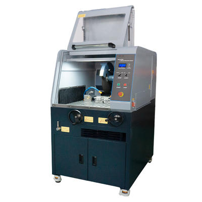
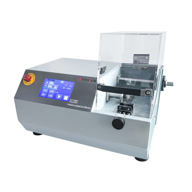
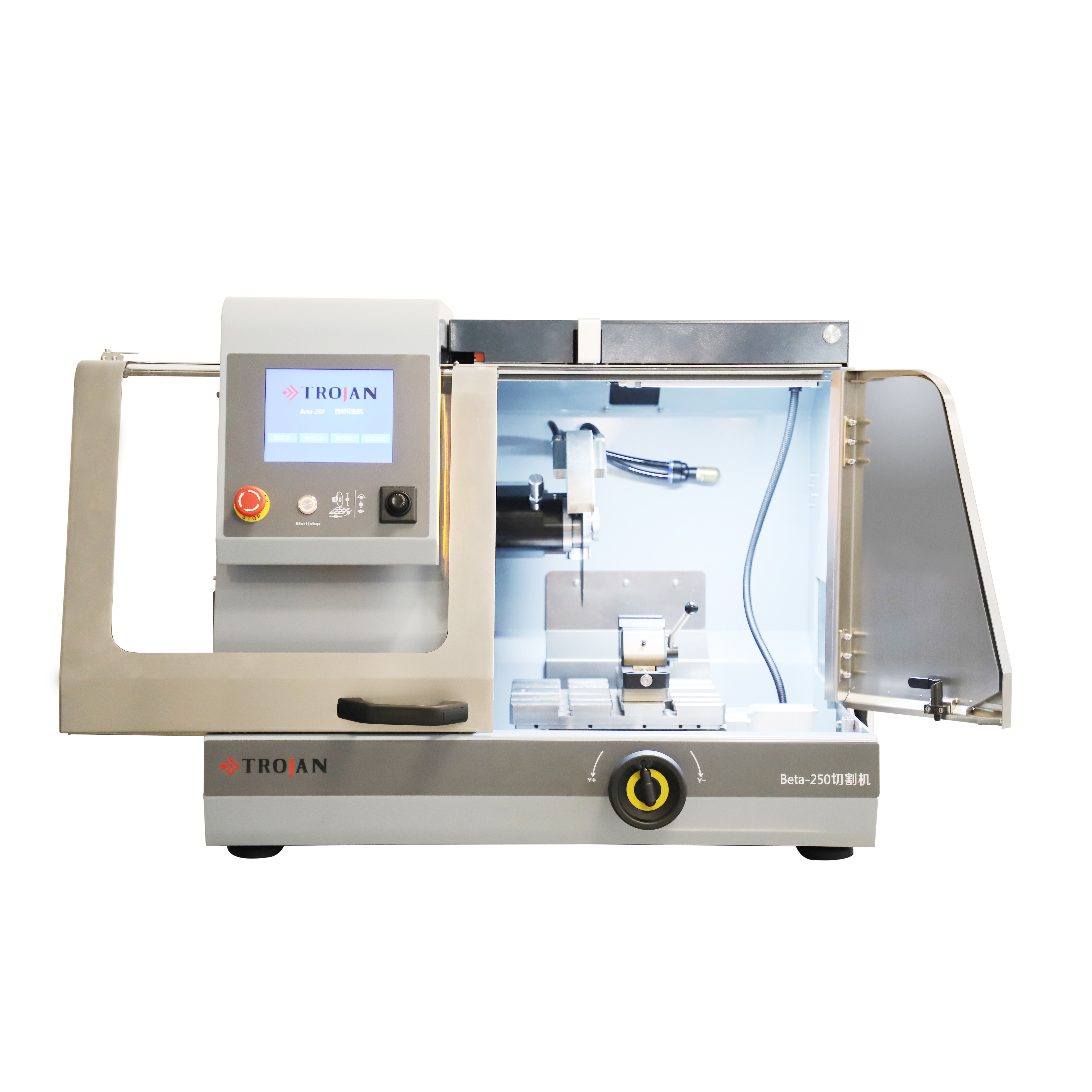


Based in China, TROJAN pays attention to the international market, and has sold metallographic equipment to more than 50 countries, such as Europe, America, Japan and South Korea, Southeast Asia countries and regions


