 英语
英语 西班牙语
西班牙语 德语
德语Abrasive Wheels
Product Description
Cuting is the first step in material analysis, and the selection of the cutting ...
We use first- and third-party cookies including other tracking technologies from third party publishers to give you the full functionality of our website, to customize your user experience, perform analytics and deliver personalized advertising on our websites, apps and newsletters across internet and via social media platforms. For that purpose, we collect information about user, browsing patterns and device.
By clicking "Accept All Cookies", you accept this, and agree that we share this information with third parties, such as our advertising partners. If you prefer, you can choose to continue with "Only Required Cookies". But keep in mind that blocking some types of cookies may impact how we can deliver tailored content that you might like.
For more information and to customize your options, click on "Cookie settings". If you want to learn more about cookies and why we use them, visit our Cookie Policy page at any time. Cookie Policy

The third-generation semiconductor power devices are mainly manufactured based on wide-bandgap semiconductor materials such as silicon carbide (SiC) and gallium nitride (GaN), and compared with traditional silicon-based devices, they have significant advantages such as large bandgap width, high breakdown electric field strength, and fast electron saturation drift speed. These characteristics enable the third-generation semiconductor power devices to operate stably under extreme conditions such as high temperature, high voltage, and high frequency, and to have higher power density, lower on-state losses and switching losses, which can effectively improve the energy conversion efficiency. Therefore, they are widely used in fields such as new energy vehicles, photovoltaic power generation, 5G communication, and rail transportation, becoming the core components that drive energy transformation and the development of high-end manufacturing industries, and are of great significance for achieving energy conservation and industrial upgrading.
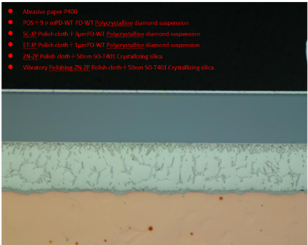
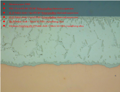
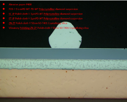
In the research and production of third-generation semiconductor power devices, the performance of the interface metal compound (IMC) layer plays a crucial role in the reliability and stability of the devices. Electron backscatter diffraction (EBSD) technology, as a powerful means of material microstructure analysis, can deeply analyze the crystallographic information, orientation distribution and phase composition of the IMC layer. However, to obtain high-quality EBSD data, sample preparation is a crucial prerequisite. The following are the metallographic sample preparation methods for your reference.
.jpg?imageView2/2/w/400/format/jpg/q/75 "Abrasive Wheels")


")


.jpg?imageView2/2/w/400/format/jpg/q/75 "PL-W Polishing Lubricants")


")
Based in China, TROJAN pays attention to the international market, and has sold metallographic equipment to more than 50 countries, such as Europe, America, Japan and South Korea, Southeast Asia countries and regions


