Chip solder balls are small spherical beads made of pure tin or tin alloys. They are used to provide electrical connection and mechanical support between chip packaging and printed circuit boards (PCBs), as well as connections between stacked packages in multi-chip modules (MCMs).
In Ball Grid Array (BGA) packaging, solder balls resolve the conflict between high pin density and miniaturization. They shorten signal paths, reduce high-frequency signal transmission loss, and enable direct thermal contact with PCBs to enhance heat dissipation efficiency. Additionally, they possess a certain degree of elasticity, which can absorb stress caused by PCB thermal expansion, reduce the risk of solder joint cracking, and improve long-term operational reliability.
Chip solder balls are widely used in chip packaging of various electronic devices, such as CPUs, SoCs, and graphics chips in smartphones, tablets, and laptops. They are also applied in the packaging of core chips in industrial control, automotive electronics, aerospace, and other fields.
Below are the sample preparation parameters for chip solder balls and an appreciation of metallographic microscopic effects:
1️⃣ Grinding: Sandpaper P400-P4000
2️⃣ Rough polishing: SC + 3μm PD-WT
3️⃣ Final polishing: ZN + 0.05nm Super
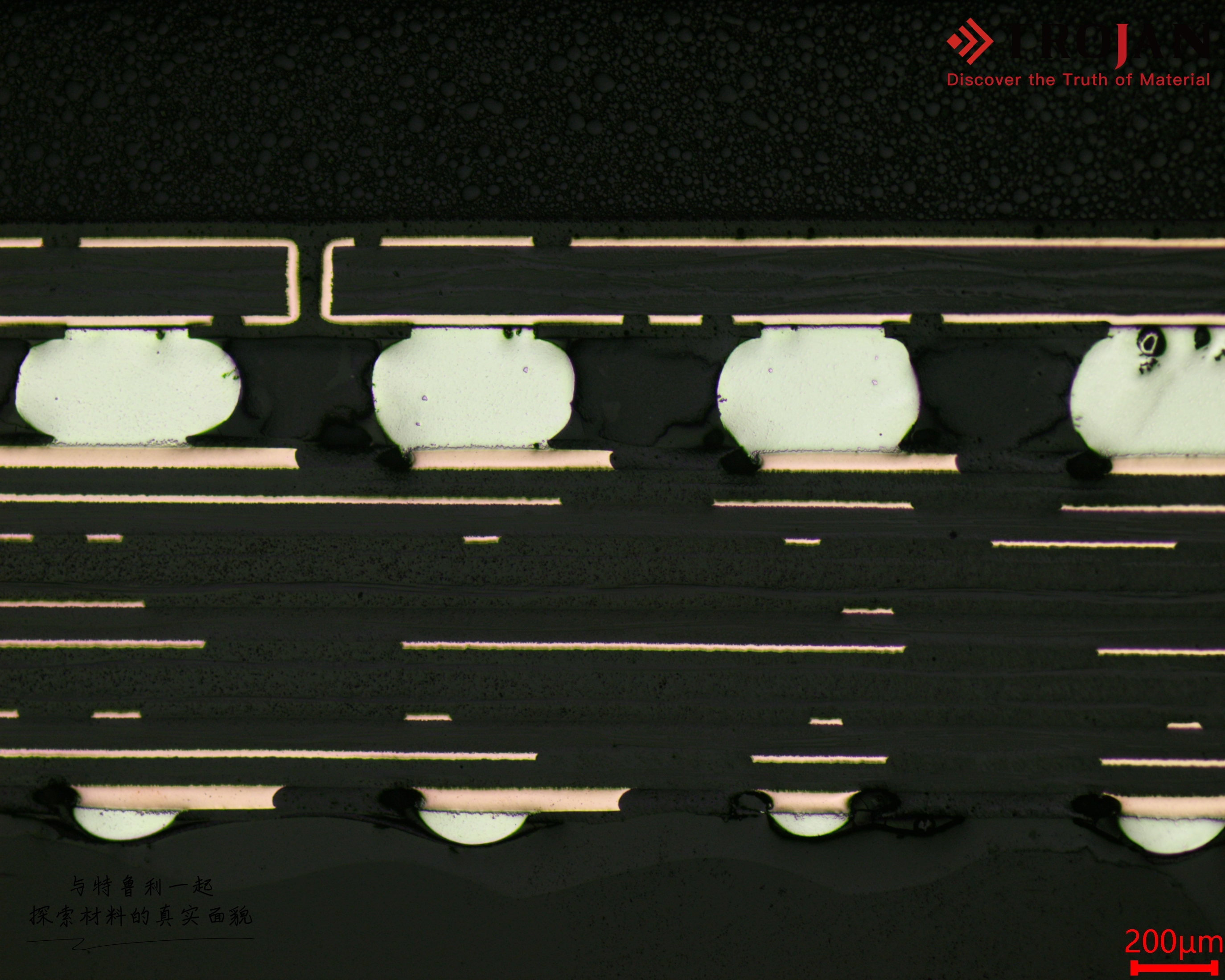
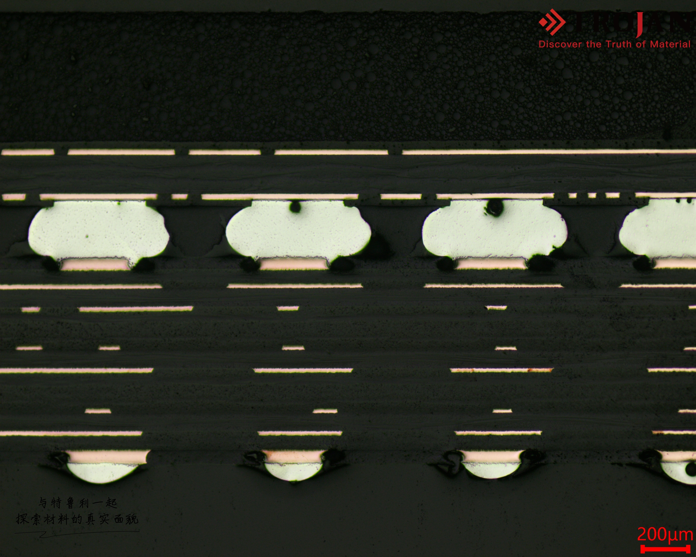
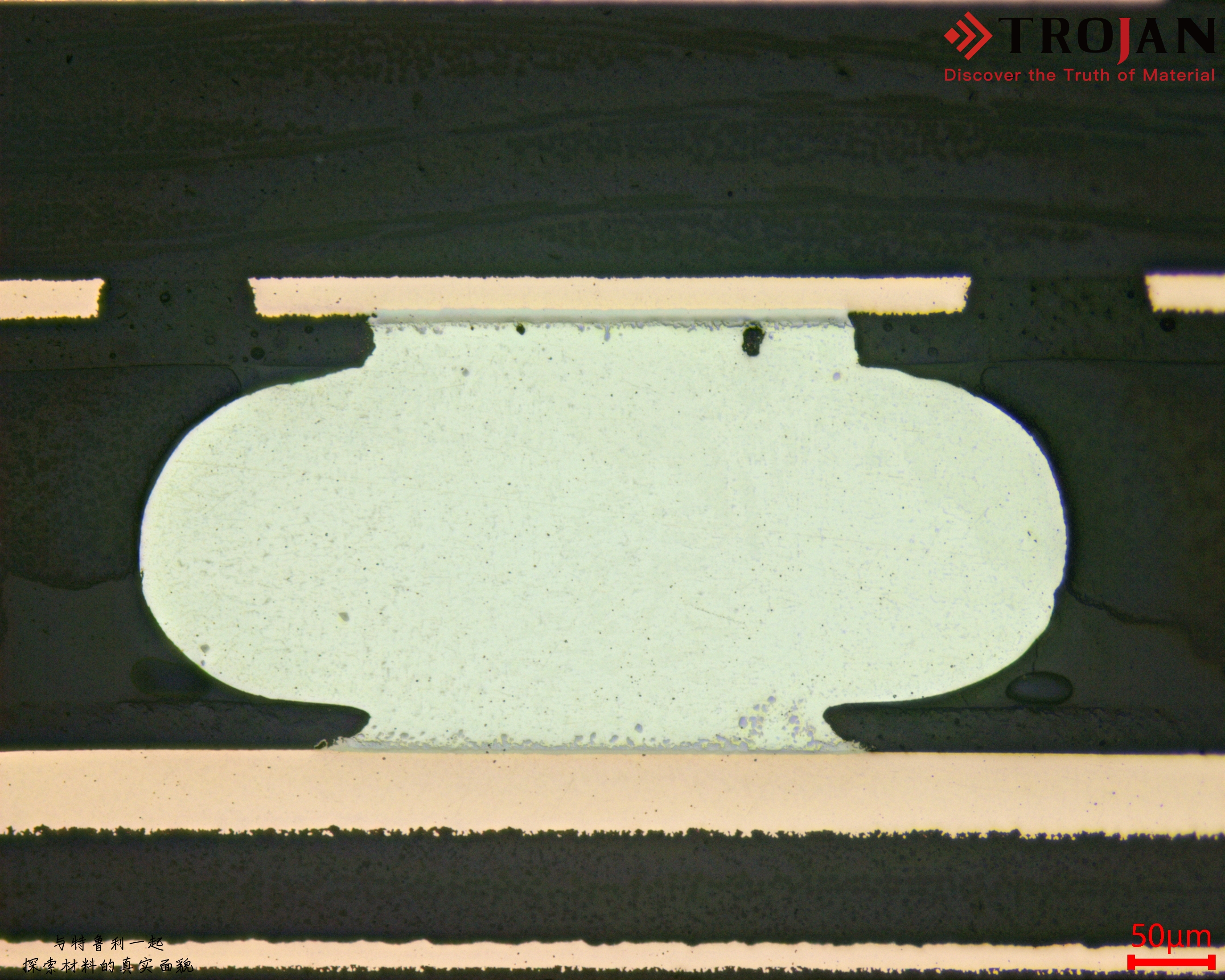
#Trojan #Trojanmetallographic #SteelMicrostructure #MaterialScience #Metallography #SteelSamples #MicrostructureAnalysis #SteelPrep #MaterialTechnician #SamplePreparation #Microscopy #MetallurgicalTesting #SteelAlloys #SteelPolishing #MicrostructureTesting #MetallographyLab #MaterialAnalysis #SteelQuality #MicroscopicView #MetallurgicalEngineering #LabTechLife #MaterialsTesting #StructuralAnalysis #metallurgymonday #crosssection #coldmounting

 英语
英语 西班牙语
西班牙语 德语
德语
