 英语
 西班牙语
 德语
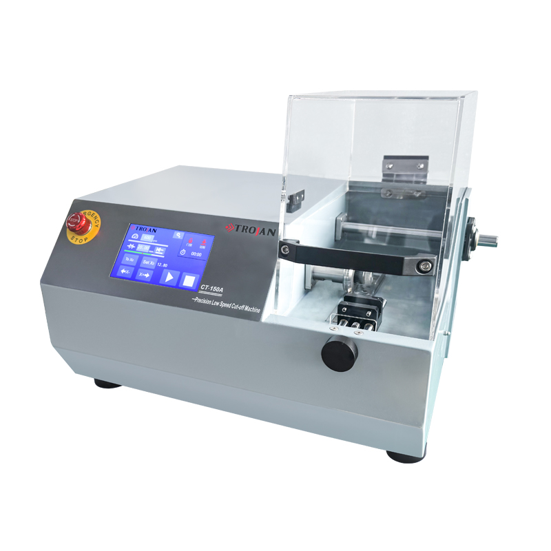
TableCUT-200 Automatic Precision Cut-Off Machine
Product Description
TableCUT-200 is automatic precision cut-off machine, equipped with various fixtu...
We use first- and third-party cookies including other tracking technologies from third party publishers to give you the full functionality of our website, to customize your user experience, perform analytics and deliver personalized advertising on our websites, apps and newsletters across internet and via social media platforms. For that purpose, we collect information about user, browsing patterns and device.
By clicking "Accept All Cookies", you accept this, and agree that we share this information with third parties, such as our advertising partners. If you prefer, you can choose to continue with "Only Required Cookies". But keep in mind that blocking some types of cookies may impact how we can deliver tailored content that you might like.
For more information and to customize your options, click on "Cookie settings". If you want to learn more about cookies and why we use them, visit our Cookie Policy page at any time. Cookie Policy

Reliability issues in microelectronic components are not always visible from the outside. Metallographic cross-sectioning is an essential technique for structural verification and failure analysis in microelectronics and SMT applications.
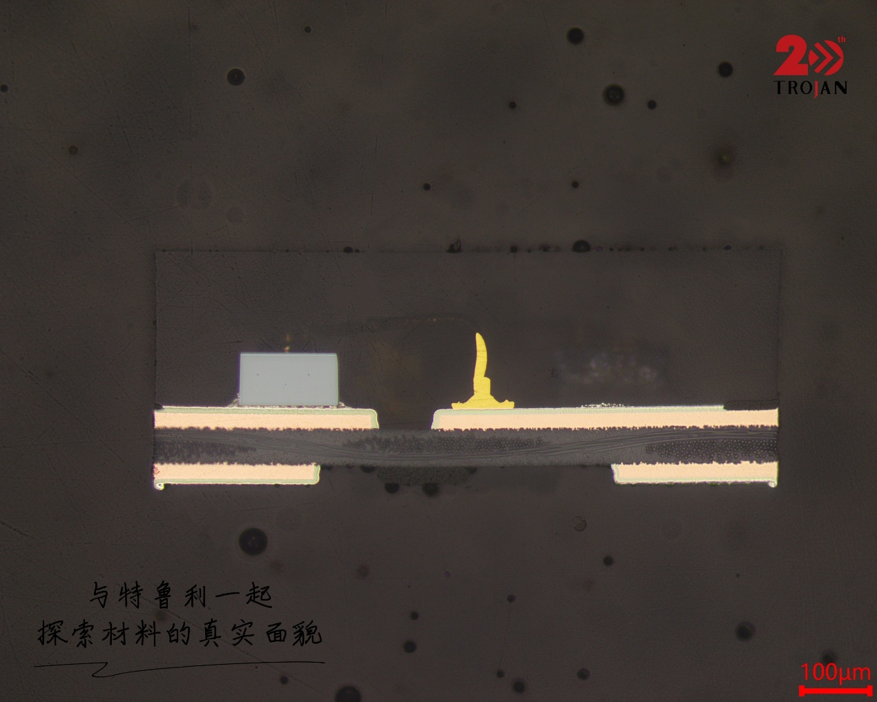
Cross-sectional examination helps evaluate several critical features:
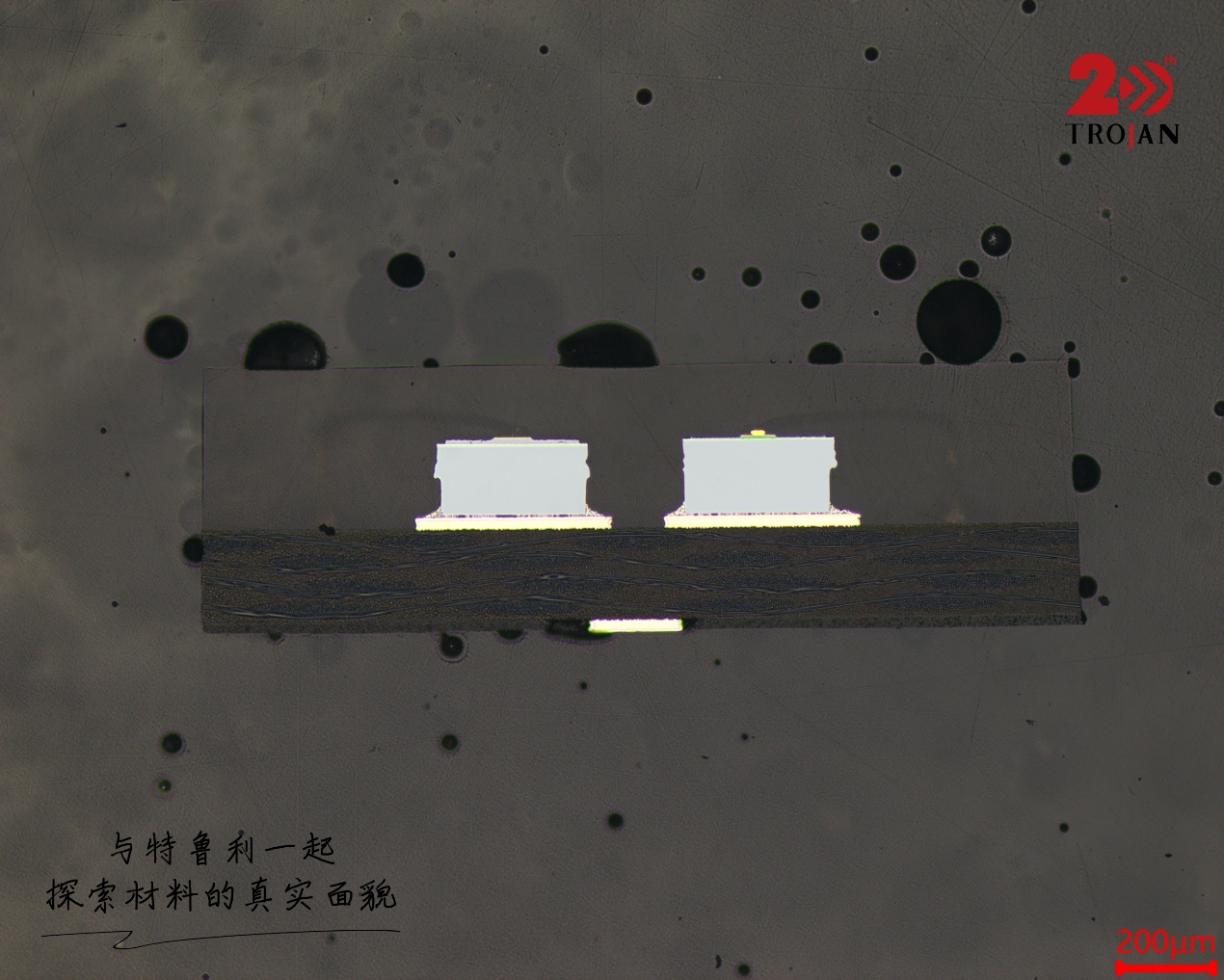
However, delicate structures such as bonding wires and die edges are particularly sensitive to preparation-induced damage. Uneven grinding pressure may cause wire smearing or edge chipping, while polishing scratches can obscure fine cracks and interface defects. Mounting resin shrinkage may also lead to separation or structural displacement.
To minimize these risks, careful process control is essential:
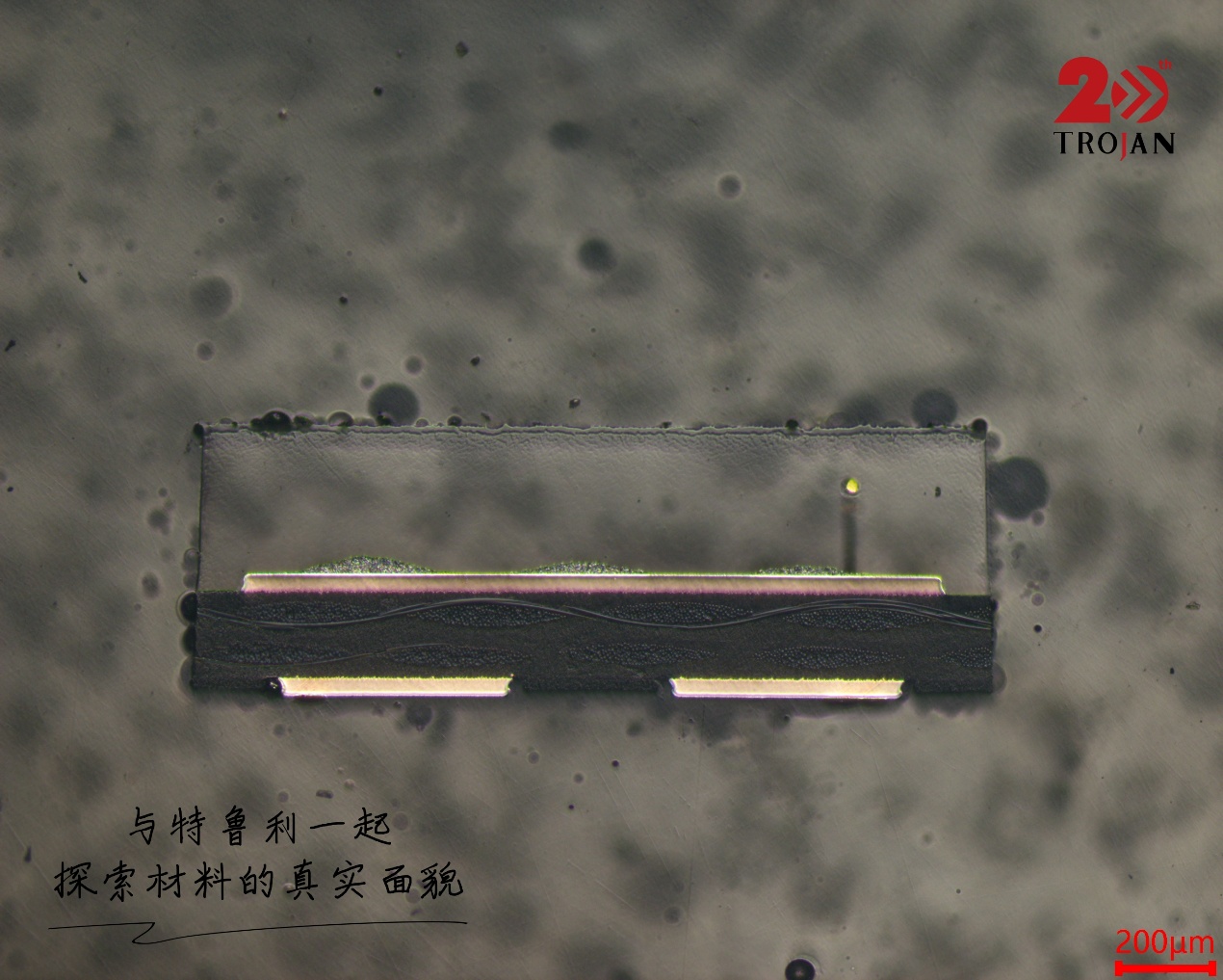
From wire bonding interfaces to die attachment structures, reliable cross-section preparation helps reveal critical details for component verification, process evaluation, and failure analysis.
Our team provides high-precision metallographic equipment and solutions tailored to your microelectronics quality verification.
Contact Us Today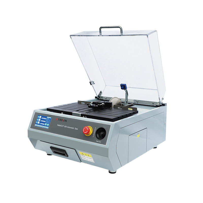




Based in China, TROJAN pays attention to the international market, and has sold metallographic equipment to more than 50 countries, such as Europe, America, Japan and South Korea, Southeast Asia countries and regions